


Breaking the “Chip” Bottleneck! SunoMeng Ultra-High-Purity Pressure Sensors: Safeguarding Every Pascal in Semiconductor Manufacturing—China’s Native Nanofilm Technology Redefines the Safety Boundaries for Special Gas Control.
2025-07-28
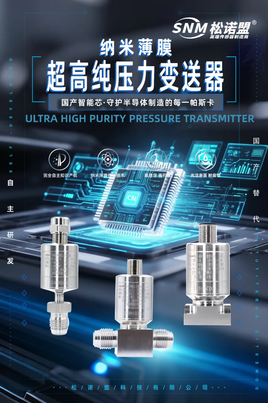
In the face of the increasingly severe situation of the U.S. escalating its semiconductor technology blockade against China, China’s chip industry is engaged in a life-or-death struggle—one that hinges on “millimeter-level precision” and “supply-chain security.” The key to success in this battle lies not only in core equipment such as lithography machines but also in achieving independent control over countless intricate manufacturing processes. Among these, stable pressure control under ultra-high-purity environments represents an often-overlooked yet critically important “invisible threshold” in semiconductor manufacturing.
01 The “Invisible Threshold” in Semiconductor Manufacturing: The Ultimate Challenge of Pressure Control
As the cornerstone of the modern technology industry, semiconductor manufacturing pursues extreme precision in every process step—from wafer processing and lithography to etching, thin-film deposition, and packaging and testing—all of which must be carried out in an ultra-high-purity environment that is nearly exacting. Even minor fluctuations in pressure parameters can, at best, lead to non-uniform thin films or deviations in etching rates, and at worst, directly result in the scrapping of an entire batch of wafers—making them a “silent killer” hindering yield improvement. Particularly in the front-end processes, the precise control of ultrapure, highly toxic, and highly corrosive specialty gases such as SiH₄, PH₃, AsH₃, ClF₃, and HF places near-extreme demands on pressure sensors:
Zero-pollution guarantee: Components that come into contact with gases must be of the highest purity, completely free from any leaching of metal ions, particles, or organic substances that could contaminate the process gases.
Excellent corrosion resistance: It can stably and reliably resist the corrosion of highly corrosive special gases such as HF and ClF₃ over the long term, thereby preventing transmitter failure or fatal leaks.
Millisecond-level responsiveness: Real-time capture of instantaneous changes in gas flow to ensure uniform etching and consistent deposition rates.
Strong electromagnetic interference resistance: Maintain stable and reliable signal output in the complex electromagnetic environment of a Fab facility.
Safety redundancy design: It is imperative to prevent the risk of toxic and flammable gas leaks, safeguarding the Fab’s assets worth hundreds of billions of yuan and ensuring the safety of personnel.
Long-term service stability: Minimize calibration frequency and downtime maintenance to ensure continuous, reliable operation and reduce overall costs.
Traditional pressure sensors often become “stumbling blocks” to yield improvement and hidden risks to safe operation due to issues such as insufficient material purity, poor corrosion resistance, and long-term drift. Under the backdrop of lockdowns, these challenges have further highlighted their role as a “bottleneck.”
02 Independent Innovation Breaks the Impasse: The Sensor Nobleman S270 Series Overcomes Challenges in Semiconductor Pressure Measurement
In response to the stringent demands of pressure control in semiconductor manufacturing, Sunno-Mate has launched the S270 series of ultra-high-purity pressure transmitters, centered around its independently developed nanofilm technology. This product breaks through traditional performance bottlenecks, achieving a seamless integration of ultra-high purity, precise measurement, and long-term stability, thereby providing a critical, self-reliant and controllable measurement solution for China’s domestic semiconductor industry chain.
The Eight Core Technological Advantages of Sensor Nobleman
1. Special alloy materials
The core pressure sensor and main structural components of the S270 series ultra-high-purity pressure transmitters from Sensor Nobleman are both made of highly corrosion-resistant alloy materials. Combined with specialized internal treatment technologies, these components can effectively resist erosion by most specialty gases, thereby eliminating at the source any risk of metal ion contamination.
2. Exceptional surface cleanliness
The surface finish reaches Ra ≤ 0.13 μm (class 10 or higher), effectively reducing particle precipitation and adsorption, perfectly meeting the requirements for ultra-high-purity gases and ensuring the purity of process gases.
3. Extremely low helium leak rate
High-intensity sealed welding with a helium leak rate ≤ 10⁻¹⁰ Pa·m³/sec (He), effectively eliminating leakage risks and meeting stringent sealing standards for demanding vacuum and ultra-high-purity environments.
4. Ultimate stability and durability
Advanced nanofilm sensing material technology and atomic-layer deposition technology deliver exceptional long-term stability.
Active temperature compensation technology ensures extremely low temperature drift over a wide temperature range (-40℃ to as high as 250℃), making it suitable for the high-temperature operating conditions of semiconductor equipment.
Million-cycle pressure life verification reduces calibration maintenance and enhances overall equipment utilization.
Special steel-based thin-film technology offers a wide measurement range (0~0.1~...~20 MPa) and flexible applications.
5. Excellent EMC stability Certified with multiple standards (CE, RoHS) to ensure the device operates safely and reliably.
6. Robust and reliable, suitable for harsh environments:
IP67-rated protection—unafraid of dust and moisture intrusion in outdoor and industrial environments.
Compact design, easily accommodating installation in the limited space inside equipment.
7. Precise measurement, stable support:
Equipped with a self-developed nano-film pressure sensor core, it offers multiple accuracy levels—±0.2%FS, ±0.5%FS, and ±1.0%FS—to meet the requirements of various application scenarios.
Equipped with a zeroing function, facilitating on-site calibration and debugging.
The entire product manufacturing process is carried out in a cleanroom, ensuring high safety, high quality, and stringent delivery standards for our products.
8. Domestic substitution of equipment Compatible with mainstream international semiconductor equipment interface protocols, helping to ensure supply chain autonomy and controllability.
03 Why choose Sensor Nobleman?
“Not just a pressure transmitter—rather, it’s a **double safeguard** for both yield and safety.”
✓ Material Purity: Exceeds SEMI F20 standard, with purity matching aerospace-grade specifications.
✓ Technical specifications: Helium leak rate, temperature range, and accuracy all surpass international competitors.
✓ Domestic Genes: Deeply understand the pain points of local manufacturing and significantly boost customization and development speed—04 Call to Action: Let domestically produced sensors safeguard China’s “chip” lifeline!
At 1:30 p.m. on July 30, Lei Weiwu, Chief Scientist of Sunno Alliance, invites you to join us for the Semiconductor Special Session at the Smart Manufacturing Conference!
Major Release: "Technical Advantages of Nanofilm Pressure Sensors and Their Applications in the Semiconductor Industry"

Book an on-site consultation now to get a personalized solution >>
Precision manufacturing begins with stability down to the smallest fraction of a millimeter. Choose pressure sensors truly designed for semiconductors, and let every pascal become the cornerstone of your competitive edge.


Contact Us
Address : No. 18 Xiangtai Road, Liuyang Economic and Technological Development Zone, Building A5, Changsha E Center.China
Phone : +86-400-002-1378
Email : business@chnsnm.com
Sales : +86-173-7371-3251 (Mr. Zeng)

Here is placeholder text for Heading 1 h1.
Service Hotline
Address: Building A5, Changsha E Center, No. 18 Xiangtai Road, Liuyang Economic and Technological Development Zone.China