


Sunno Alliance cordially invites you to join us at the 2025 Shanghai International Semiconductor Technology Exhibition! Let’s jointly build the cornerstone of sensing technology and empower a new ecosystem for the semiconductor industry!
2025-07-17
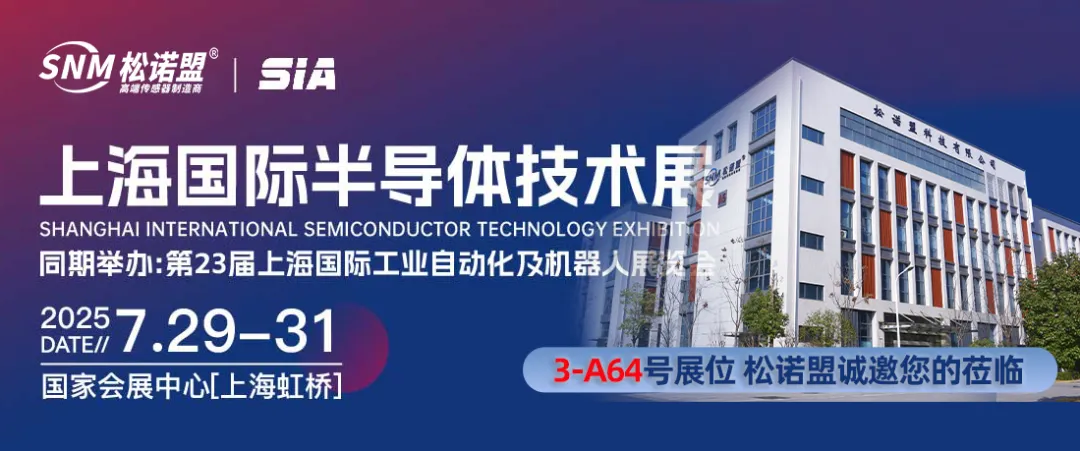
Key Value of the Exhibition: A “Weather Vane” for the Global Semiconductor Industry
As a prestigious, specialized brand event for the semiconductor industry at the national and global levels, the 2025 Shanghai International Semiconductor Technology Conference & Exhibition will be held from July 29 to 31 at the Shanghai National Exhibition and Convention Center. The exhibition focuses on identifying and showcasing innovative products, technologies, solutions, and business collaboration models in the semiconductor industry, providing a one-stop solution for semiconductor companies to promote their brands, display their products, and foster exchanges and cooperation—thus helping semiconductor and related enterprises achieve comprehensive, end-to-end communication and connectivity across the entire industry chain.
✅ Exhibition Scale: This exhibition covers over 71 countries, with an expected exhibition area of 60,000 square meters, more than 1,000 exhibitors, and is anticipated to attract over 100,000 professional visitors.
✅ Panoramic showcase of 6 cutting-edge technology zones: Wafer Fabrication | Packaging & Testing | Compound Semiconductors | Automotive Semiconductors | EDA/IP Design | Key Components (with a focus on the Sensor Core Zone)
✅ Directly covering 8 hot application fields: Smart Cars | Industrial Automation | 5G Communications | New Energy | Robotics | High-End Equipment | IoT | Military Electronics
✅Bringing together global industry decision-makers: Providing a one-stop platform for brand promotion, technology collaboration, and supply chain matchmaking.
Sunno Alliance’s Core Technology: Infusing Semiconductor Manufacturing with “Precision Sensing”
The semiconductor industry is booming, and technological innovation is the core engine driving its future. On the path toward higher yields, more precise manufacturing processes, and smarter production, accurate sensing is a crucial link in breaking through bottlenecks.
As a leading domestic supplier of high-end sensor solutions, Suno-Ming Technology Co., Ltd. has been deeply rooted in the industry. At this exhibition, we’re bringing our innovative, high-performance nanofilm semiconductor pressure sensors, injecting powerful “precision sensing capabilities” into semiconductor manufacturing. We cordially invite you to visit the 2025 Shanghai International Semiconductor Technology Exhibition (National Exhibition and Convention Center, Booth No. 3-A64) and join us in exploring how sensor technology can drive the transformative upgrade of semiconductor manufacturing!

✨ Cutting-edge technology empowers the upgrade of intelligent manufacturing.
Relying on its deep technological expertise, Sensor Nobleman focuses on addressing the challenges of high-precision measurement and stringent environmental monitoring in semiconductor manufacturing. Its core strengths lie in:
Nano-film technology: stable and reliable—high-performance semiconductor pressure sensors manufactured using cutting-edge nano-film technology offer high measurement accuracy and excellent stability, providing reliable and precise pressure measurements for semiconductor processes such as wafer fabrication, thin-film deposition, precision lithography, and vacuum annealing.
Real-time control in harsh environments: To meet the demand for real-time monitoring of process environments, our nanofilm pressure sensors can operate stably under extreme conditions—including high temperatures, high purity, highly corrosive media, and hazardous atmospheres—accurately measuring pressure parameters and ensuring process stability and consistency.
✨ Cutting-edge products, unveiled live!
In the demanding semiconductor manufacturing process, pressure measurement is not only critical for accuracy but also essential for ensuring the purity of gases and media. At our booth, we’ll be showcasing the next-generation pressure sensors specifically designed for semiconductor manufacturing—the CYB-S270 series ultra-high-purity pressure transmitters. These transmitters are specially engineered to handle ultra-high temperatures, ultra-high-purity gases, and harsh process environments, enabling you to achieve truly reliable pressure monitoring.

The product’s core strengths focus on semiconductor demand:
1. Exceptional surface cleanliness (critical!):
- It employs a highly corrosion-resistant alloy material combined with specialized internal treatment technology.
- Surface finish reaches Ra ≤ 0.13 μm (class 10 or higher), effectively reducing particle precipitation and adsorption, perfectly meeting the requirements for ultra-high-purity gases and ensuring the purity of process gases.
2. High-strength sealed welding Helium leak rate ≤ 10⁻¹⁰ Pa·m³/sec (He), eliminating the risk of leakage and meeting stringent sealing standards for demanding vacuum and ultra-high-purity environments.
3. Ultimate stability and durability:
- Advanced nanofilm sensing material technology and atomic-layer deposition technology deliver exceptional long-term stability.
- Active temperature compensation technology ensures extremely low temperature drift over a wide temperature range (-40℃ to as high as 250℃), making it suitable for the high-temperature operating conditions of semiconductor equipment.
- Special steel-based thin-film technology offers a wide measurement range (0~0.1~...~20 MPa) and flexible applications.
4. Robust and reliable, suitable for harsh environments:
- IP67-rated protection—unafraid of dust and moisture intrusion in outdoor and industrial environments.
- Compact design, easily accommodating installation in limited spaces within equipment.
- Outstanding EMC stability and multiple certifications (CE, RoHS) ensure the device operates safely and reliably.
5. Precise measurement, stable support:
- Offers multiple accuracy levels—±0.2%FS, ±0.5%FS, and ±1.0%FS—to meet the requirements of various application scenarios.
- Equipped with a zeroing function, facilitating on-site calibration and debugging.
- The entire product manufacturing process is carried out in a cleanroom, ensuring high safety, high quality, and stringent delivery standards for our products.
Solution experts, jointly tackling industry challenges.
To help you gain a comprehensive understanding of the latest developments and technological advantages of nanofilm pressure sensors, Lei Weiwu, Chief Scientist at Sunon Alliance, will deliver a special presentation titled “Technological Advantages of Nanofilm Pressure Sensors and Their Applications in the Semiconductor Industry” at the Smart Manufacturing Solutions Conference for the Semiconductor Industry on July 30 at 1:30 p.m. You’re welcome to join us for this engaging discussion and exchange.
Sunno Alliance fully understands that each manufacturing stage presents unique measurement challenges. During the exhibition, our team of seasoned technical experts will be on-site throughout the event, engaging in face-to-face, in-depth discussions with you and providing a detailed analysis of innovative application cases for sensors in advanced manufacturing processes—such as advanced packaging and compound semiconductors.
We precisely identify the measurement challenges you face in yield improvement, process control, and equipment maintenance, and tailor the optimal sensor solutions to meet your needs. This helps you optimize your production processes, enhance manufacturing efficiency, and boost product competitiveness.
Looking forward to meeting you and jointly crafting a “chip”-based future.
Every leap in precision in semiconductor manufacturing is underpinned by the robust support of sensing technology. SunoMinds is committed to being your key partner on the path to process upgrades, offering ultra-precise sensor products and professional, reliable technical services!
From July 29 to 31, at Booth A64 in Hall 3 of the Shanghai National Exhibition and Convention Center, Sunno Alliance will be waiting for you—let’s explore together how sensing technology can empower the future of semiconductors!


Contact Us
Address : No. 18 Xiangtai Road, Liuyang Economic and Technological Development Zone, Building A5, Changsha E Center.China
Phone : +86-400-002-1378
Email : business@chnsnm.com
Sales : +86-173-7371-3251 (Mr. Zeng)

Here is placeholder text for Heading 1 h1.
Service Hotline
Address: Building A5, Changsha E Center, No. 18 Xiangtai Road, Liuyang Economic and Technological Development Zone.China